
The Aixtron Series | Part 1: Power Electronics
Aixtron's business model, the SiC glut and China bear case, and the Nvidia 800VDC GaN bull case

Hello and welcome to my Substack! Updating this about 45 days since it was published as there are many new readers to whom I want to introduce my writing and publishing style.
This will be part 1 of 3 on my series for this company. This first part covers the background, business model, and the bull case for power electronics: SiC and GaN. Part 2 will focus mainly on optoelectronics and will also feature a finished revenue build. Part 3 will detail Aixtron’s criminally underrated financials, walking through a three-statement model and DCF.
Without further ado, lets dive right in.
Introduction
In a nutshell, Aixtron is a semicap (semiconductor capital equipment) company. Semicap companies sell equipment to chip fabs to manufacture chips. Aixtron specializes in equipment for a very niche process called epitaxy.
Epitaxy
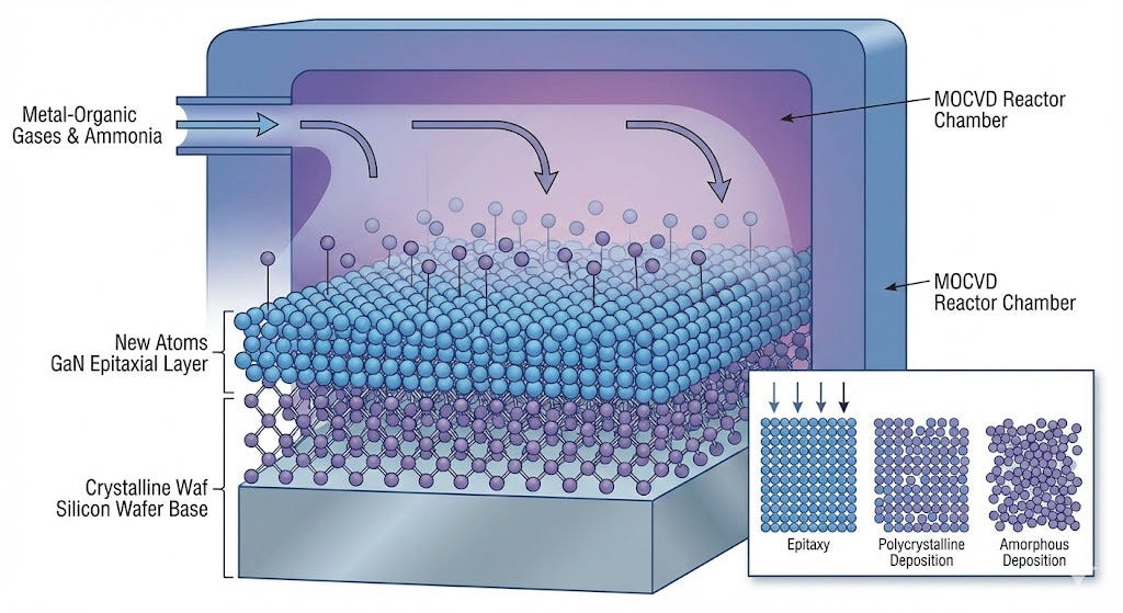
To understand that, we first have to talk about Deposition, one of the many steps in the complicated semiconductor manufacturing process. Deposition is essentially like baking a very complicated lasagna—it’s all about layers. You start with a base (the wafer), and then you stack different materials on top of it to conduct or block electricity. The act of putting those layers down is called Deposition. Usually, you pump some gas into a chamber, it reacts, and it settles as a solid film on the wafer.
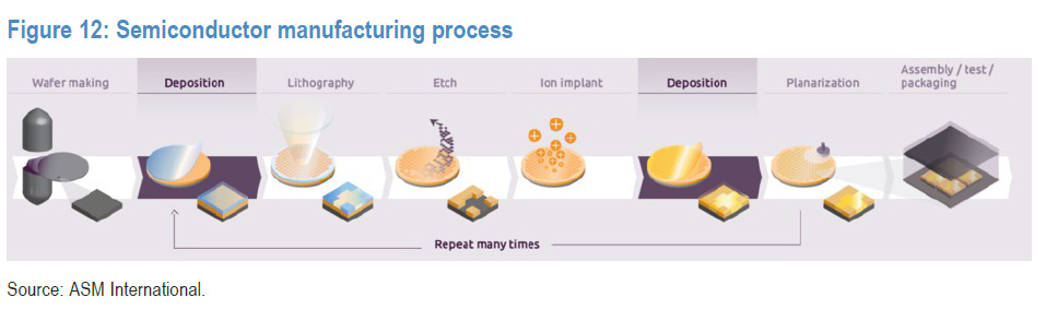
However, Aixtron doesn’t just do “normal” deposition. They do the really hard stuff: Epitaxy.
In standard deposition, you can sometimes get away with just spraying material onto the wafer like graffiti on a wall. It doesn’t matter if the atoms land sideways, upside down, or in a jumbled pile. But for the high-performance chips Aixtron deals with, “jumbled” means the chip is dead on arrival.
Epitaxy is Atomic Tetris.
When Aixtron’s tools deposit a layer, the new atoms can’t just land anywhere. They have to line up perfectly with the crystal structure of the layer below them. They need to lock into a specific grid pattern, extending the perfect crystal structure upwards. If a few atoms are out of place—if your Tetris tower has a gap or a crooked piece—the chip goes in the trash.
Aixtron builds the machines that control heat, pressure, and gas flow with such insane precision that these crystals grow perfectly, atom by atom, every single time. It is the step that determines whether you have a supercomputer chip or a very expensive paperweight.
The following graphic sums up how tetris-like epitaxy differs from standard deposition.
End Markets
Aixtron reports in four distinct segments split by end market:
Gallium Nitride (GaN)
Silicon Carbide (SiC)
Optoelectronics
LED.
These are four distinct types of semiconductors, each playing a specific role in the modernization of power and connectivity.
Gallium Nitride (GaN) and Silicon Carbide (SiC) are both classified as power electronics. Power electronics are chips that control electricity. These chips manage the conversion of voltage and current, turning high-voltage power from the grid into the kind of energy that machines can use. They live inside EV inverters, solar and wind farms, chargers, and the racks that feed power-hungry GPUs. Wide-bandgap materials like gallium nitride (GaN) and silicon carbide (SiC) are revolutionizing this space, replacing legacy silicon components because they can switch faster, handle higher voltages, and waste less energy as heat.
Gallium Nitride (GaN) is the efficiency specialist of the group. While legacy silicon chips struggle with heat and size as power demands rise, GaN excels at switching electricity at incredibly high speeds with minimal energy loss. You likely already own a GaN chip inside a compact fast-charger for your phone or laptop.
Silicon Carbide (SiC) is the heavy lifter. Like GaN, it is a wide-bandgap material designed to replace silicon, but its superpower is handling brute force—extreme voltages and scorching temperatures that would destroy a standard chip. This makes SiC the standard-bearer for heavy industrial applications and automotive power.
Optoelectronics encompasses the chips that control light. These components serve as the physical bridge between the electronic and optical worlds, converting electricity into light (lasers) or light back into electricity (detectors). This segment is critical because light carries vastly more information than electrons—moving faster, with less energy loss, and at much higher bandwidth. This technology powers the 3D sensors that let cars see their surroundings and the FaceID on your phone, but its most critical role today is as the nervous system of the AI buildout, powering the lasers that move massive amounts of data across hyperscale data centers.
Finally, LED is the display segment. While most people associate this with the commoditized red-orange-yellow LEDs used in traditional signs you might see outside stores at night, Aixtron’s involvement here is increasingly focused on the next technological leap: MicroLED. This represents the future of high-end displays for smartwatches and augmented reality devices, promising screens with perfect color accuracy and brightness that far exceed current OLED technology. While currently a smaller part of the growth story compared to Power and Opto, it remains a potent call option on the future of consumer hardware.
Aixtron’s Business Model
Aixtron’s business model blends cyclical hardware sales with a recurring service component. Roughly 80% of its revenue comes from selling new equipment, while the rest comes from after-sales servicess. Equipment demand rises and falls with the semiconductor cycle, but the installed base grows steadily, creating a stable stream of service revenue that smooths earnings between booms.
Financially, Aixtron operates with gross margins around 40%, while operating margins typically sit near 20%. The fixed cost structure gives it meaningful operating leverage: When orders rise, earnings rise much faster, and when orders slow, profits compress. Product mix plays a role as well: new GaN and AsP tools command premium margins, while older LED tools drag the average down.
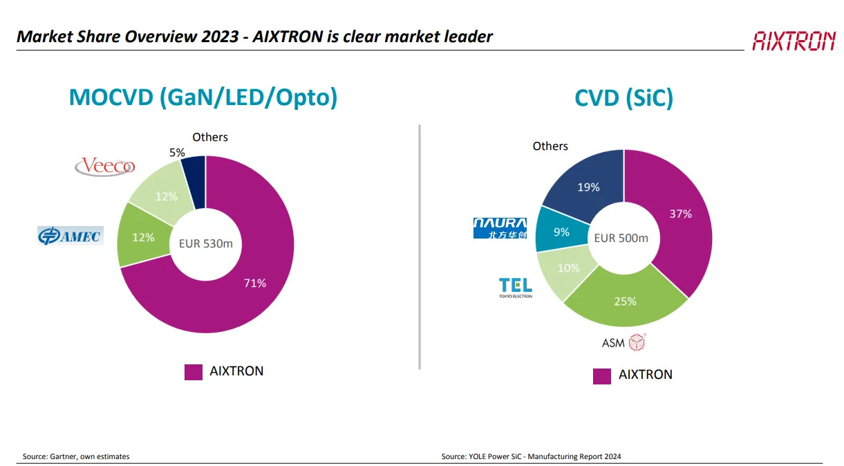
In its core market of MOCVD systems for compound semiconductors, Aixtron controls roughly 70–75% share globally. Its closest competitors are Veeco in the U.S. and AMEC in China, but neither has matched Aixtron’s combination of scale, process stability, and breadth across power and optical applications. In SiC CVD tools, its position is smaller, about one-third of the market, where it competes primarily with ASM International and LPE.
The Semicap Equation
Semiconductor capital equipment follows a surprisingly elegant mathematical logic. It can be written as:
E(t) = R(t) + k × dW(t)/dt
Where:
E(t) represents total equipment demand at time t — the revenue drivers for companies like Aixtron, ASML, or Lam Research.
R(t) is replacement demand, the base level of tool purchases needed to replace aging equipment. This grows slowly with the installed base but lags by roughly 7–10 years.
k is a proportionality constant capturing how strongly equipment orders respond to changes in wafer output growth. It differs across technologies; compound semiconductors often have a higher k because capacity ramps are discrete and lumpy.
W(t) is wafer output — the total manufacturing capacity of chips at a given time.
dW(t)/dt is the first derivative of wafer output, which measures the rate of change of chip production.
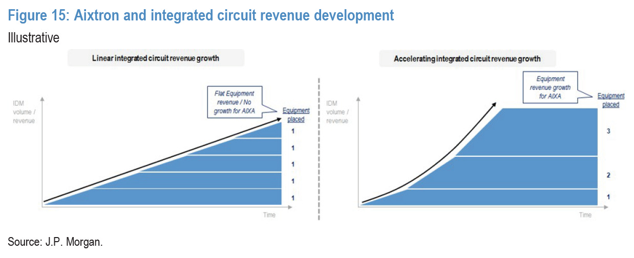
Semicap is a derivative of end-market growth—literally. Equipment sales are the derivative of wafer output: they only grow when wafer capacity accelerates. If wafer production increases at a steady, linear rate, chipmakers simply use their existing tools a bit longer; equipment demand stays flat. True growth occurs when the industry’s output accelerates.
Replacement demand does exist but it moves slowly, growing with the installed base on a 7–10-year lag as tools age out of production. In theory, if the semiconductor industry was mature, R(t) would grow as the installed base grows, making semicap growth proportional to wafer growth. However, since semis are a fast-growing industry, this replacement effect is small relative to the expansionary cycles. That makes R(t) insignificant relative to dW(t)/dt, meaning that semicaps often undergrow their respective end market wafer demands.
Hated by the Sell Side
With 12 hold ratings and as many sells as buys, Aixtron is hated by the sell side. At 8x FY2 EBITDA (with a prior average of ~16x), Aixtron is hated by the market too. There are three good reasons why.
Limited Future Growth
The sell side’s core issue with Aixtron is that growth looks capped for the next year and a half. After a historic boom in 2021–2023, when EV and renewable energy OEMs raced to add silicon carbide (SiC) and gallium nitride (GaN) capacity, the industry is now glutted. Overinvestment during that period built too much installed base and left customers digesting excess tools. Utilization rates have dropped, and fabs that were supposed to expand again in 2024–2025 are now pausing to absorb what they already bought.
The order book tells the same story. Aixtron’s backlog has stagnated and is gradually drifting lower, a clear sign that the tool cycle has entered a holding pattern. JPMorgan argued that consensus numbers are still too high because they embed a continuation of mid-cycle growth that simply isn’t there. They expect a wave of downward revisions once earnings catch up with the reality of flat order intake. In the near term, Aixtron’s revenue growth will track analog and power semiconductor capex, which the bank sees falling in 2025 versus 2023–2024 before a modest recovery later on.
Meanwhile, the P&L optics worsen before they get better. With volumes flat, operating leverage reverses, and the cost base built during the 2021–2024 expansion now weighs on margins. Higher depreciation and amortization from the new Herzogenrath R&D center and Turin factory add roughly a point of EBIT pressure, and a mix shift away from high-margin SiC tools toward LED and optoelectronics compresses profitability further. JPMorgan estimates 2025–2026 EBIT margins could come in 10–15% below current consensus.
Competition
Aixtron faces pressure from both Western and Chinese competitors. In China, domestic equipment makers like AMEC, TOPEC, Naura, and JSG are rapidly improving their deposition tools, supported by state-backed industrial policy that explicitly favors local suppliers. The Chinese government’s “buy local” mandates and the capital from the Big Fund have accelerated qualification programs for homegrown epitaxy equipment.
Meanwhile, in the U.S. and Europe, rivals are resurging. Veeco, once written off, has re-entered GaN power and laser tools; ASM International bought LPE, giving it a stronger position in SiC CVD.
With SiC and GaN demand in digestion mode, there’s little growth to offset pricing pressure. JPMorgan’s base case already bakes in slight share loss in both Western and Chinese markets, reflecting what it sees as a “normalized” competitive landscape after the easy-share-gain years of 2021–2023. Margins could come under pressure if Aixtron cuts prices to defend its install base, and its heavier R&D reinvestment (about 15% of revenue) makes the optics worse in a flat-growth environment.
China
Roughly one-quarter of total sales come from China. That used to be a blessing, given the region’s strong growth, but may soon become a curse. The country’s massive government fund continues to support compound semiconductor buildouts, creating near-term demand. However, as is characteristic with the Chinese market, the government encourages overinvestment without regard for ROIC, inevitably resulting in gluts. This is a real risk. China leading demand growth cannot be sustainable if the demand is artificial and the installed base becomes too large.
—
However… There is one catalyst that may change everything.
Nvidia 800V HVDC Rack Architecture
The Current Architecture
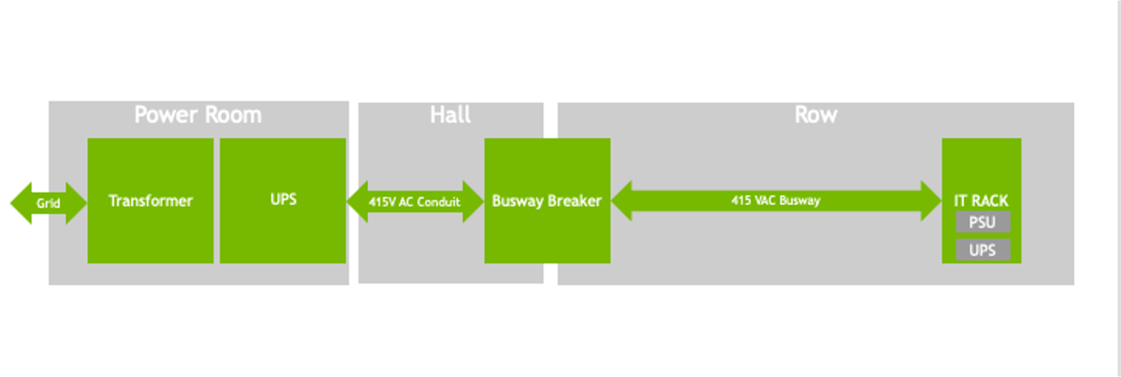
Electricity begins its journey into a data center the same way it reaches a neighborhood, through the utility grid as medium-voltage alternating current (AC), typically between 35 and 110 kilovolts. AC is ideal for long-distance transmission because it carries large amounts of power efficiently, but computers can’t use it directly. Therefore, inside the data center, transformers first step that power down to 415 or 480 volts AC, which is routed through power-distribution units (PDUs) and busbars that feed rows of server racks. At this stage everything is still AC, optimized for movement rather than computation.
Once the electricity reaches a rack, the AC/DC conversion process begins. Each rack contains power-supply units (PSUs) that act as the first conversion stage, taking the incoming AC power and turning it into 54 volts direct current (DC), the format electronic components require. This is known as the front end. From there, the DC travels through the rack to each server tray, where a second layer of converters known as intermediate bus converters (IBCs) further step the voltage down. In today’s systems that usually means dropping from roughly 400–800 volts DC to 48 volts, and then to 12 volts before the power reaches the compute boards. Inside the tray, the final step happens at the chip level. A network of miniature DC-to-DC converters takes that 12-volt input and feeds the GPUs, CPUs, and memory modules with ultra-precise voltages often between one and five volts.
Each stage of this process creates conversion loss as heat. The result is an end-to-end efficiency of less than 90 percent, meaning more than a tenth of the facility’s total energy is lost before computation even begins. Engineers call the first stage the front end (AC-to-DC at rack entry) and the second the intermediate bus converter, which performs the successive DC-to-DC reductions. The front end (AC-to-DC at rack entry) relies mainly on silicon or silicon-carbide (SiC) devices built for high voltage and reliability, while the intermediate stage depends on faster, high-frequency materials, a distinction that sets the stage for why Nvidia’s 800-volt redesign matters for Aixtron.
The Scale Problem
The race to train ever-larger AI models is reshaping the physics of the data center. Each new generation of GPU delivers more performance, but also demands far more power. A higher-power rack is faster: Packing more GPUs into a single rack shortens communication distance between chips, cutting latency and enabling those GPUs to act as one enormous processor. The result is exponential performance gains: moving from 32 to 72 GPUs in a single domain can yield 50× more compute throughput even if power only rises 3–4×. In the world of large-language models, where milliseconds of delay compound over trillions of operations, that density directly translates into faster training and greater utilization of capital. The problem is that every step up in compute density multiplies the load on the electrical system supporting it.
That brings us to the limits of today’s power distribution. A conventional rack running at 54 volts can comfortably handle a few dozen kilowatts. Push it to 200 kilowatts and the math breaks. Power equals voltage times current, so if voltage stays fixed, current has to rise. At these levels the currents are enormous, requiring busbars as thick as wrists, heavy copper cables, and oversized connectors. The more current you push, the more heat you generate, and the more energy you lose in transmission. Data centers are already wasting double-digit percentages of their electricity as conversion loss and heat; doubling or tripling current makes those inefficiencies explode. Beyond a few hundred kilowatts per rack, the old 415-volt AC and 54-volt DC architecture becomes physically and economically unworkable.
There’s another constraint: volatility. AI workloads don’t draw power smoothly. When thousands of GPUs operate in unison, power demand can swing from 30 % to 100 % utilization and back in milliseconds. These swings ripple through the facility, forcing engineers to oversize every link in the chain (PSUs, PDUs, even the grid interconnect) to handle the peaks. The cost of this over-engineering shows up as stranded capacity and higher per-watt capital expense.
Why HVDC Transition Is Inevitable
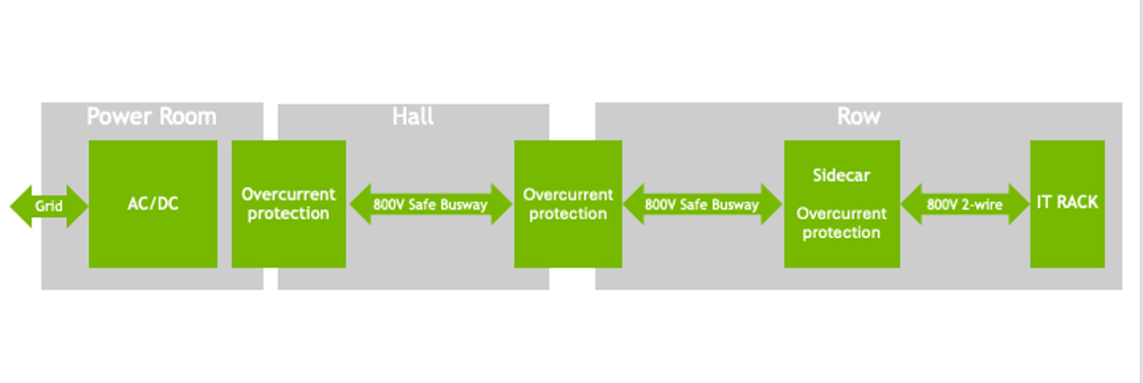
In May, NVIDIA released their next generation Kyber rack architecture. Instead of distributing alternating current (AC) at 415 V or low-voltage direct current (DC) at 54 V, Kyber converts power from the grid’s medium-voltage AC to 800 V DC once at the facility level and then distributes it directly to each rack. Inside the rack, a single high-ratio DC-DC converter—a 64:1 LLC converter positioned right beside the GPUs—steps that voltage down to 12 V, which then feeds the chips through short traces and local regulators. By centralizing AC-to-DC conversion upstream and minimizing conversion stages inside the rack, Kyber turns the power architecture of a data center from a complex tree of converters into one streamlined, high-voltage trunk.
In the legacy model, power enters the rack as low-voltage AC, then cascades through multiple PSUs and converters before reaching the processors, losing efficiency and creating heat at every step. In Kyber, nearly all of that intermediary hardware disappears. The rack itself becomes a direct DC endpoint and the GPUs receive clean, stable 12 V DC power through a much shorter and simpler path.
The payoff is profound. An 800 V DC system transmits the same power with roughly one-seventh the current of a 115 V or 54 V system, dramatically cutting resistive losses and copper usage. Because the distribution voltage is higher, the conductors are thinner, the heat output is lower, and the cooling demand drops in tandem. Beyond efficiency, Kyber directly addresses the volatility problem: The architecture integrates multi-timescale energy storage, with capacitors near the racks to absorb millisecond-level spikes and larger batteries at the facility to buffer seconds-to-minutes fluctuations. The result is a power system that scales to megawatt racks, operates cooler and cheaper, and stabilizes the grid rather than stressing it.
Why GaN is Inevitable and How Aixtron Benefits
The 800-volt architecture will change what materials power it. The heart of Nvidia’s Kyber rack is the 64:1 IBC that drops voltage from 800 V down to roughly 12 V right beside the GPU. This converter must handle enormous instantaneous currents, switch at megahertz frequencies, and maintain flawless efficiency inside a space barely larger than a paperback book. That’s exactly where gallium nitride (GaN) excels. Its crystal structure allows electrons to move faster and with lower capacitance than either silicon or silicon carbide (SiC), which means GaN transistors can switch far more quickly and with less loss. The faster the switching, the smaller the magnetics and cooling hardware required. SiC, by contrast, shines at the front end of the system (high voltage, low-frequency conversion) but its larger die size and slower switching make it inefficient and bulky in the IBC stage.
Because Kyber’s design standardizes that single, high-power, high-frequency conversion stage, GaN content per rack increases dramatically. Each rack contains multiple GaN-based modules managing power delivery to dozens of GPUs. For Aixtron, this shift is transformative. GaN devices are manufactured using MOCVD, a process where Aixtron commands about 71% market share. SiC devices, by contrast, use CVD, where Aixtron’s share is closer to 37%. That means every dollar of semiconductor production migrating from SiC to GaN represents disproportionate incremental revenue for Aixtron. GaN epitaxy is capital-intensive, since each dollar of device output requires mid-single-digit percentages of tool capex. In conclusion, Aixtron is the primary picks-and-shovels beneficiary of this architectural transition.
Up Next
Revenue and gross margin models and why optoelectronics is the hidden gem.
Very interesting. I came into SiC in 1990s. So seen SiC go from research to (real) market. Since 2010 my focus is optoelectronics and photonics. There will be a second generation of applications.
Really well written posts!